Results
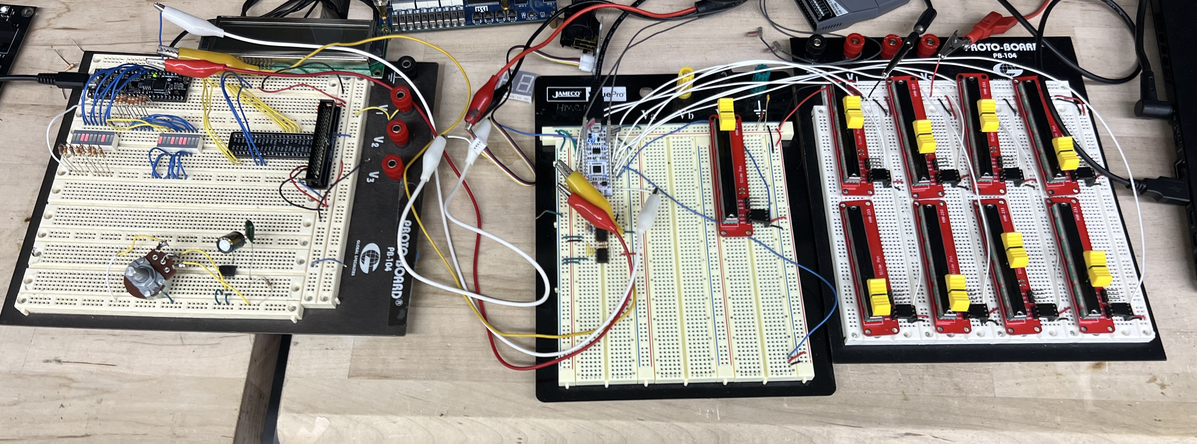
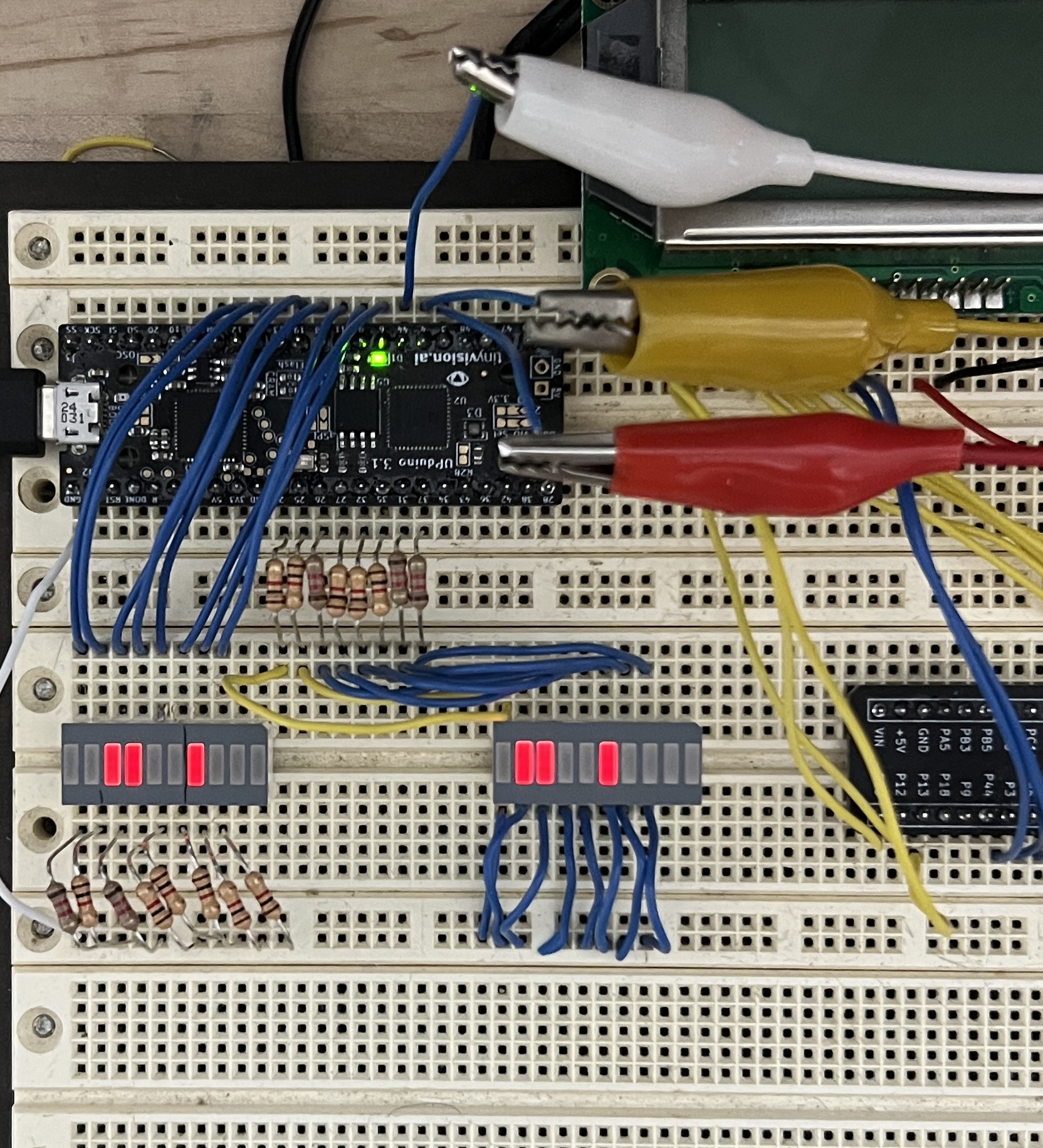
Our implementation as of the due date of this assignment was mostly successful. The DMX controller worked as intended with no perceivable latency, and although the data transmitted to the FPGA was not displayed on an LCD as intended, it was successfully transmitted and received and could be viewed in binary on an LED display.
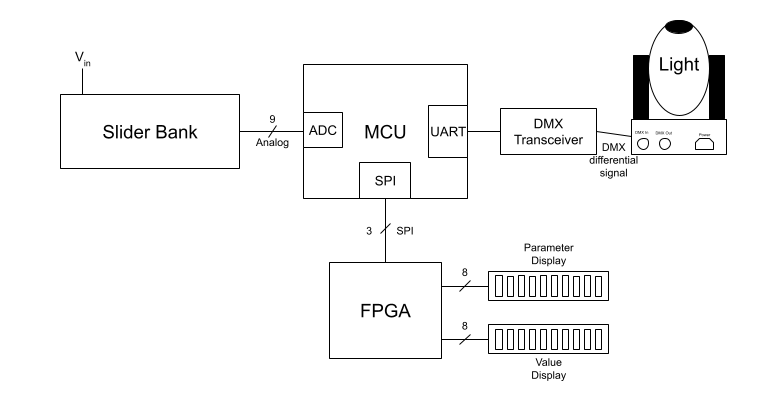
The modified block diagram with the LED displays instead of the LCD is below
To determine the latency of the control board, we measured the time between DMX signals on the oscilloscope. Since the DMX transmission is part of the main loop, a new signal is only sent after all the parameters have been updated.
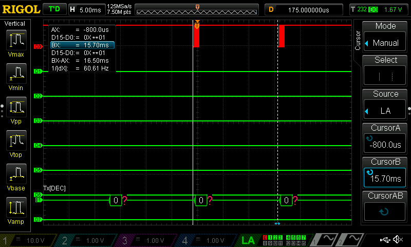
As you can see from the cursors, the time between transmissions is only 16.5ms, which is too small for people to perceive.
The time from changing a value to it displaying on the FPGA display is roughly the same. The SPI communication occurs at 20MHz, but it only happens once every loop.
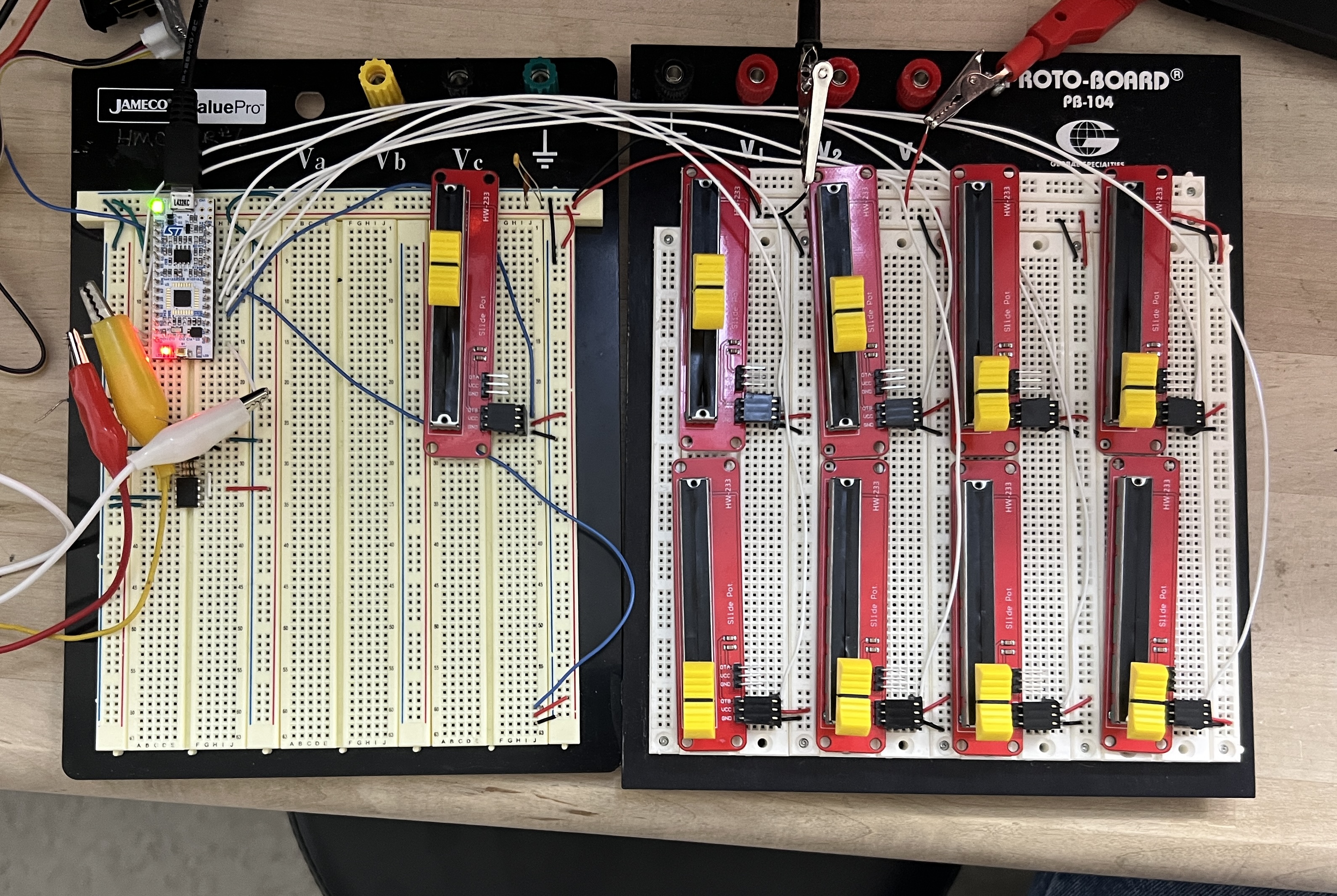
The Hardware implementation is quite barebones, though we have plans to improve it outside the timescale of this course. The sliders are mounted to a breadboard as shown below.
##Simulations
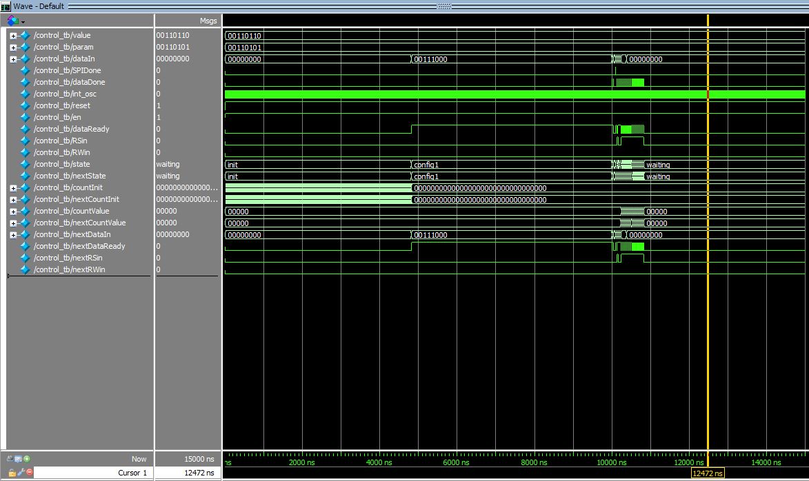
Although we never got the LCD screen to work, we could fully simulate the correct functionality of the LCD control FSM, as shown in the picture below.
