FPGA Design
Overall Design
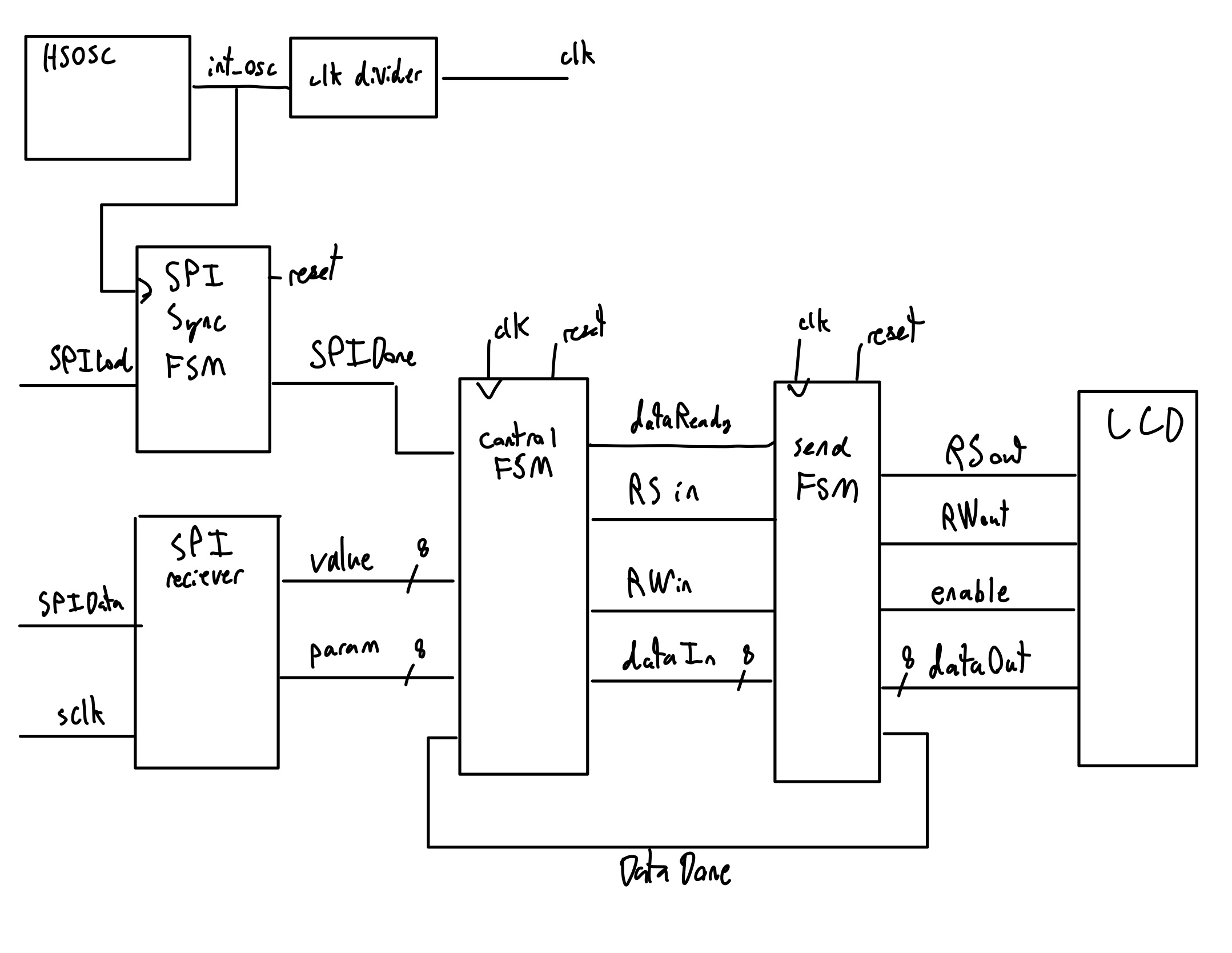
The FPGA system is responsible for receiving SPI data from the MCU and displaying this data on a 16x2 LCD display. This SPI data contains the DMX parameter number and the current value of the most recently changed parameter. The FPGA then uses a combination of different modules and finite state machines to implement the LCD protocol and display the SPI data visually on the screen. This design was adapted from a previous E155 Project by Declan O’Neill and Kip Macsai-GorenBelow is the HDL block diagram. Note, the IO for the FPGA is spread across four units on the schematic.

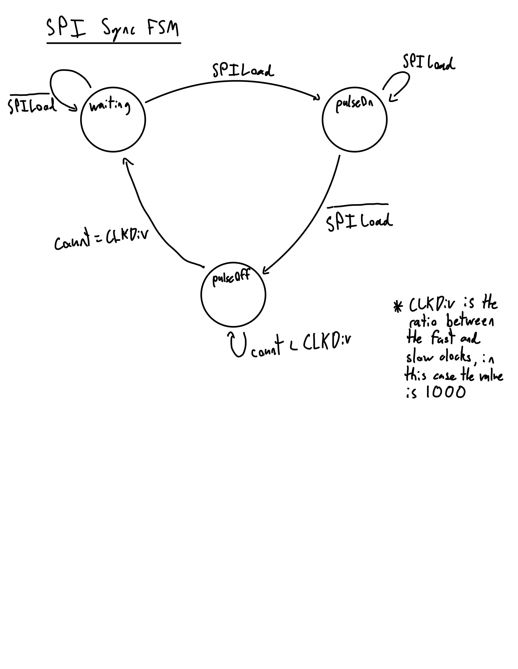
This design begins with an SPI receiver module that accepts the SPI data from the MCU and organizes it into two 8-bit signals. One signal represents the parameter number and the other represents the value of that parameter. The system also receives an SPILoad signal that indicates an SPI transaction is happening. This signal is sent through a synchronizer FSM to ensure that an SPIDone signal is held high for long enough to be detected by the slower 20kHz clock of the control FSM. This pulse is held high for 1000 clock cycles, as this is the ratio between the fast and slow clocks. This ensures that the slow clock can detect the SPIDone signal. This synchronizer is shown below.

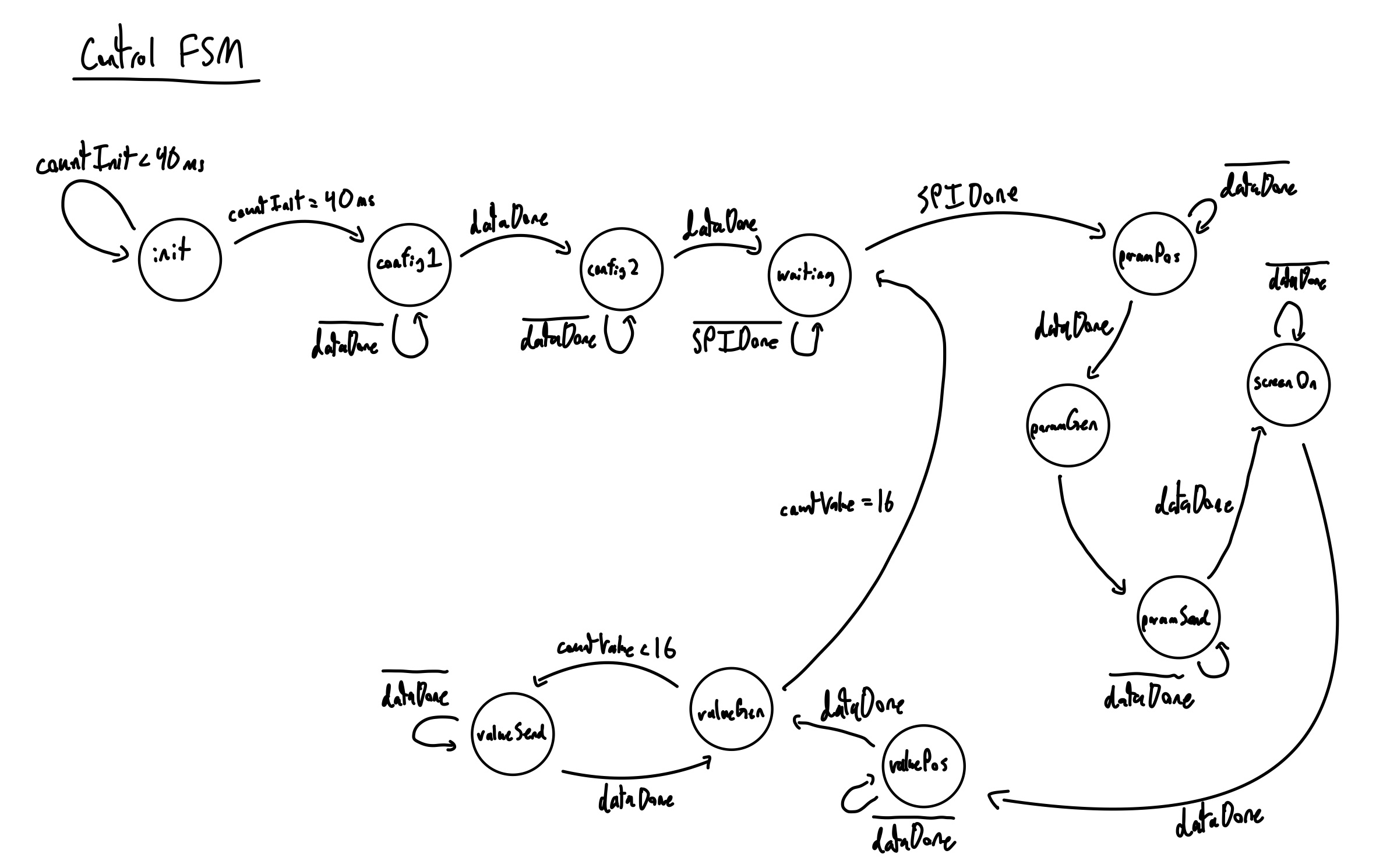
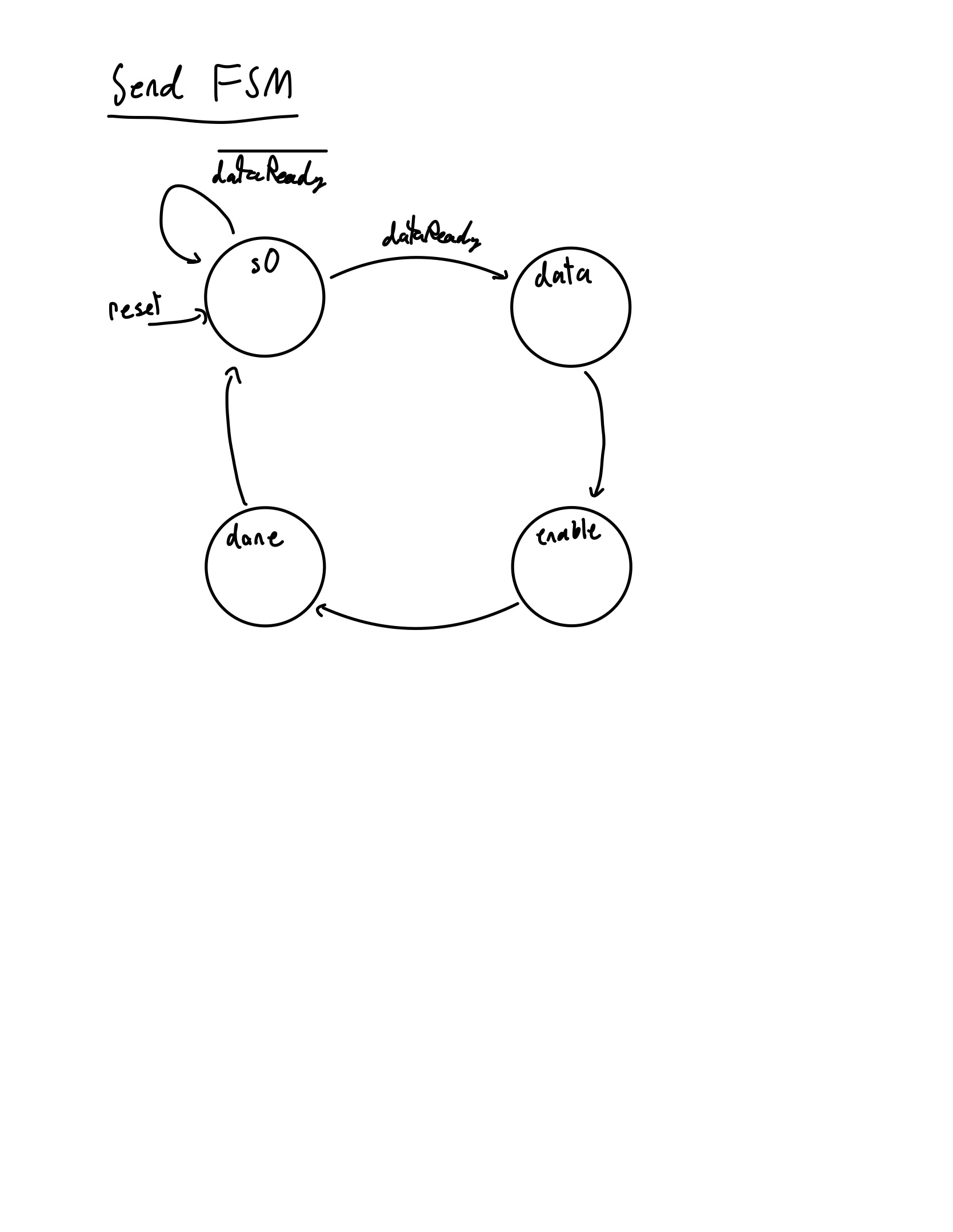
The biggest and most important FSM of this design is the control FSM. On startup, this FSM sends specific values to the configuration register of the LCD screen. This puts the screen into a mode where the cursor is automatically incremented after each character is written. The FSM then waits to receive the SPIDone signal from the synchronizer to indicate when the SPI data transaction is finished. The FSM then sets certain values for the RW, RS, and data signals to correctly display the value and param on the LCD screen. For each set of data to be sent to the screen, the FSM raises a dataReady flag to indicate to the final sending FSM that the data is ready to be sent to the screen. The sending FSM then raises a dataDone flag to indicate when the data transfer is complete. State transition diagrams for the control FSM and the sending FSM are shown below


Unfortunately, as mentioned in our results, the LCD screen was not included in the final implementation of the project, but we instead displayed the binary values of the value and param signals on 16 LEDs. The control FSM is very complex with many different pieces that all need to work together perfectly for success. Although it worked in simulation, we were never able to get it working in hardware.